With the addition of a state-of-the-art research facility, Penn’s vision for eastward expansion is being realized.
The designs for the Krishna P. Singh Center for Nanotechnology — which has been eight years in the making — were approved Thursday at the Facilities and Campus Planning Trustee Meeting.
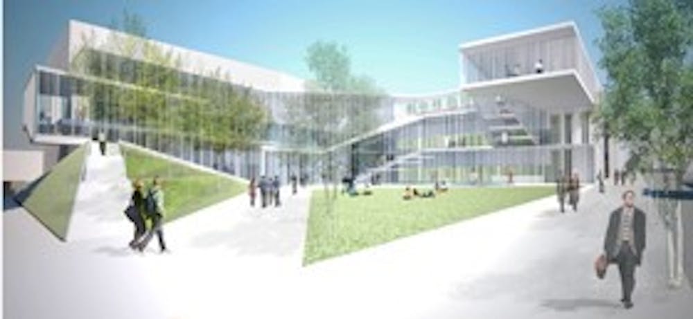
The construction for the $80 million center, which will be located on the north side of the 3200 block of Walnut Street, will most likely begin in the fall of 2010 and last approximately 26 months, according to Director of Design and Construction Chris Kern.
“The School of Arts and Sciences has identified nano-science as a priority for future investment,” SAS Dean Rebecca Bushnell wrote in an e-mail.
“We have scientists across departments in SAS doing ground-breaking work in this field, and to produce their best work they need access to the best possible facilities,” she wrote.
The purpose of the center is to foster “a collaborated effort” between the scientists in the SAS and the scientists in the School of Engineering and Applied Science, Vice Dean of SAS Ramin Sedehi said.
“This site is a prime gateway location for Penn,” Vice President of Facilities and Real Estate Services Anne Papageorge said.
“We see this building and this site as an opportunity to really enhance our gateway and to create a more welcoming connection to Center City.”
The architectural and design firm Weiss/Manfreidi and the engineering and construction firm M+W Zander were selected on the basis of nanotechnology and design experience, according to University Architect David Hollenberg.
The center will be constructed through a “fast-track shelling process,” according to Executive Director of Design and Construction Mike Dausch. This means that the outside “skin” of the building will be constructed initially and the interior portion of the building will be added later, Papageorge added.
The center will have four main components: microscopy labs, 10,000 square feet of environmentally controlled clean rooms, general labs and optics labs for research and collaboration spaces, Kern said.
The center will feature prominent green elements, which will evoke a sense of unity with Penn’s other major sites, like the College Green and the Palestra, Hollenberg said.
“One of the unique features of this building is that it is transparent and has views into labs which have more traditionally been private spaces for researchers and scientists,” Papageorge said. “That’s a really great way to open up the science of nanotechnology to the broader community.”
The project’s leaders are pursuing the LEED Silver certification, and “we are quite confident that this will easily make silver and some are hoping for more,” Hollenberg said.
“This center is indispensable for prototyping new devices for the next wave of nanotechnology creation, which the campus is lacking,” Dean of SEAS Eduardo Glandt said. “It will have an iconic presence [at] the University, and it will be revolutionary for the University and for the region.”
